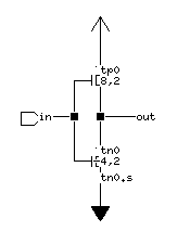
![[Decoder Schematic]](decoder.gif)
Titlepage | Introduction | Overview | Datapath | Layout | Testing | Conclusion | References.
The Basic Microinstruction sequencer (BMS) is designed to handle 8 different microinstructions. The Instruction ROM basically acts are the instruction coder and control logic for the operation of the BMS. 4 control signals are generated by the ROM based on an input of 3 bits of instruction code and 2 bits of condition code. The instruction set supported by the ROM is shown in the table below.
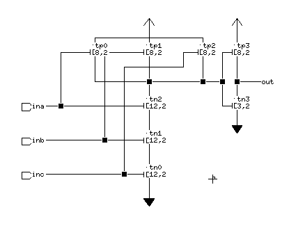
A ROM was used instead of a PLA for ECO-tolerance, since there wasn't a tight constraint on area. In the event that changed to the opcodes have to be made, it would be much simpler to modify a ROM rather than a PLA. The ROM consists of three main components: a 3-to-8 decoder, a 8-to-1 selector and a pulldown array.
|
|
|
|
Y / STACK |
Y / STACK |
|
|
|
|
|
|
|
|
|
|
|
|
|
|
|
|
|
|
|
|
|
|
|
|
|
|
|
|
|
|
|
|
|
|
|
|
|
|
|
|
|
|
|
|
|
|
|
|
The following are the schematics for the design:
The decoder is basically made up of 8 3-input AND gates each supplied with an appropriate version of the 3 input signals.
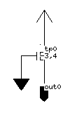
The transistor-level schematics for the individual components are available: inverter and 3-input AND-gate.
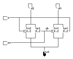
The selector is simply a chain of 4 2-input muxes driven by an inverter.
![[Selector Schematic]](selector.gif)
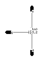
The transistor-level schematics for the individual components are available: inverter and 2-input multiplexor.
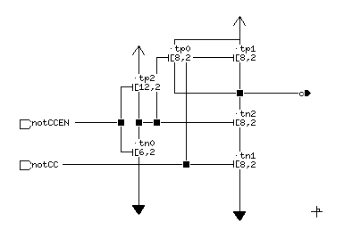
The Instruction ROM was constructed from the decoder and selector described above with a pulldown array. The coding scheme for the 4 output signals are given in the following section.
![[ROM Schematic]](rom.gif)
The schematics for the decoder and the selector are shown above, other transistor-level schematics for lower-level individual components are available: inverter, 2-input NAND-gate with one inverted input, pullup and pulldown.
|
|
|
|
|
|
|
|
|
|
|
|
|
|
|
|
|
|
|
|
|
|
|
|
|
|
|
|
|
|
|
|
|
|
|
|
|
|
|
|
Comments to benleong@mit.edu
or mike_sy@mit.edu or sclee@mit.edu
Last updated 11/21/96.
Titlepage | Introduction | Overview | Datapath | Layout | Testing | Conclusion | References.