MIPS Processor
Objective
Building a Processor
There are two major components of a processor:
- Datapath
- Collection of components that proces data.
- Performs the arithmetic, logical and memory operations.
- Control
- Tells the datapath, memory and I/O devices what to do according to program instructions.
What we are going to implement is a simplest possible implementation of a subset of the core MIPS ISA. In particular, we are interested only at the following operations:
- Arithmetic and Logical:
add,sub,and,orandiorislt. - Data Transfer:
lwandsw - Branches:
beqandbne
In particular, we will not be implementing shift instructions (i.e., sll and srl) as well as J-format instruction (i.e., j).
These are left as exercise for the reader.
Instruction Execution Cycle
Our processor will follow the typical 5 execution cycle:
-
Fetch
- Get instruction from memory.
- Address in in
$PCregister (i.e., program counter).
-
Decode & Operand Fetch
- Find out the operation required.
- Get the operand(s) needed for operation.
-
ALU
- Execute arithmetic and logical operations on ALU unit.
-
Memory
- Read/write from memory.
-
Writeback (a.k.a. Result Write)
- Store the result of the operation.
| Stage | add $3, $1, $2 |
lw $3, 20($1) |
beq $1, $2, label |
|---|---|---|---|
| Fetch | Read instruction at $PC |
Read instruction at $PC |
Read instruction at $PC |
| Decode & Operand Fetch | ∘ Read [$1] as opr1 ∘ Read [$2] as opr2 |
∘ Read [$1] as opr1 ∘ Use 20 as opr2 |
∘ Read [$1] as opr1 ∘ Read [$2] as opr2 |
| Execute | ∘ result = opr1 + opr2 | ∘ addr = opr1 + opr2 | ∘ taken = (opr1 == opr2)? ∘ target = ( $PC+4) + (label×4) |
| Memory | ∘ Use addr to read data from memory | ||
| Writeback | [$1] = result |
[$3] = mem data |
if (taken) then $PC = target |
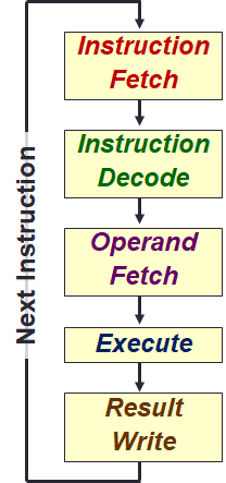
-
Fetch
- Get instruction from memory.
- Address in in
$PCregister (i.e., program counter).
-
Decode
- Find out the operation required.
-
Operand Fetch
- Get the operand(s) needed for operation.
-
Execute
- Perform the required operations, which may typically be:
- Execute arithmetic and logical operations on ALU unit.
- Read/write from memory.
-
Writeback (a.k.a. Result Write)
- Store the result of the operation.
| Stage | add $3, $1, $2 |
lw $3, 20($1) |
beq $1, $2, label |
|---|---|---|---|
| Fetch | standard | standard | standard |
| Decode | standard | standard | standard |
| Operand Fetch | ∘ Read [$1] as opr1 ∘ Read [$2] as opr2 |
∘ Read [$1] as opr1 ∘ Use 20 as opr2 |
∘ Read [$1] as opr1 ∘ Read [$2] as opr2 |
| Execute | ∘ result = opr1 + opr2 | ∘ addr = opr1 + opr2 ∘ Use addr to read data from memory |
∘ taken = (opr1 == opr2)? ∘ target = ( $PC+4) + (label×4) |
| Writeback | [$1] = result |
[$3] = mem data |
if (taken) then $PC = target |
Design
Our 5 stage comes from a design decision to:
- Merge decode and operand fetch stage (originally split).
- Since decode is simple for MIPS due to it being a fixed-length instruction.
- Split ALU and memory stage (originally merged as execute).
- Since memory is practically two operations:
- Arithmetic on the offset + base address.
- Memory access.
- Since memory is practically two operations:
You can click on "Basic" tab to see the basic cycle.
Basic Processor Design
With this introduction, we are now ready to build a MIPS processor. We are going to study the design from the viewpoint of a designer instead of a "tourist".
- Look at each stage closely and figure out the requirements as well as processes.
- Sketch a high-level block diagram then zoom in for each elements.
- With the simle starting design, check whether different type of instructions can be handled:
- Add modifications when needed (i.e., go back to step (1) for each additional instruction).