Decode Stage
Requirements
The decode stage is combined with the operand fetch stage due to the simplicity of the pure decode stage.
Pure Decode Stage
In the case of RISC such as MIPS, due to its fixed-length instruction format, the pure decode stage is very simple.
This is because the opcode is always the first 6 bits plus additionally maybe funct at the last 6 bits for R-format instruction.
On the other hand, CISC architecture may require a dedicated pure decode stage. This is because instructions may be of multiple size (e.g., 1 to 17 bytes long for Intel 80x86). Consider that we can only read 4 bytes of data from memory, if the instruction is 8 bytes long, then we need to read the instruction twice. This can only be known during the decode stage.
Since the decode stage is done after the fetch stage, it takes as its input, the output of the fetch stage. Additionally, the output of the decode stage will be passed to the ALU stage.
-
Read the
opcodeto determine the instruction type and field lengths. -
Read data from all necessary registers.
- Can be two registers (e.g.,
add,sub,beq, etc). - Can be one register (e.g.,
addi,lw, etc). - Can be zero register (e.g.,
jbut our processor do not support this).
- Can be two registers (e.g.,
-
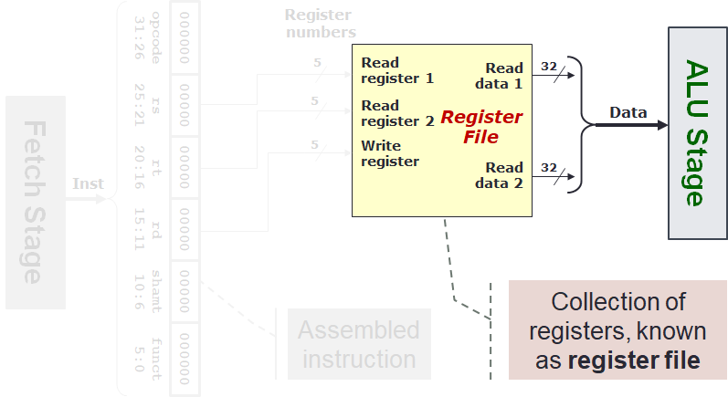
The data read is given as output to the next stage (i.e., ALU stage).
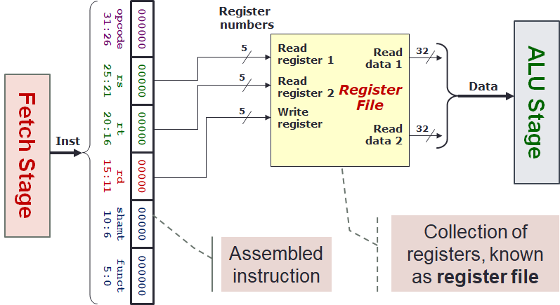
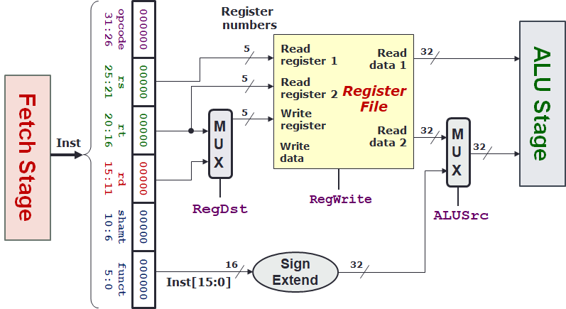
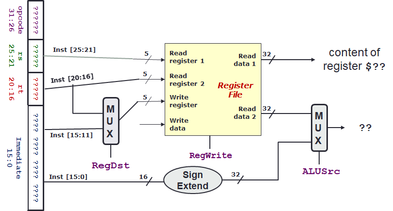
Block Diagram
Given the requirements above, we can have the following initial design:
As usual, let us take a look at the three steps more closely. We will later note that this initial design will not satisfy certain operations. This will be replaced with a more correct design later.
Steps
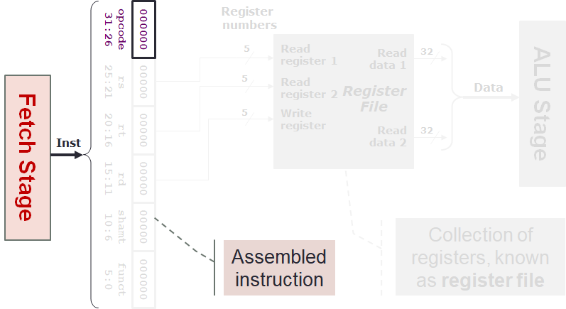
The instruction is passed from the fetch stage.
The opcode is at bit 26 to 31 (i.e., 6 bits MSB).
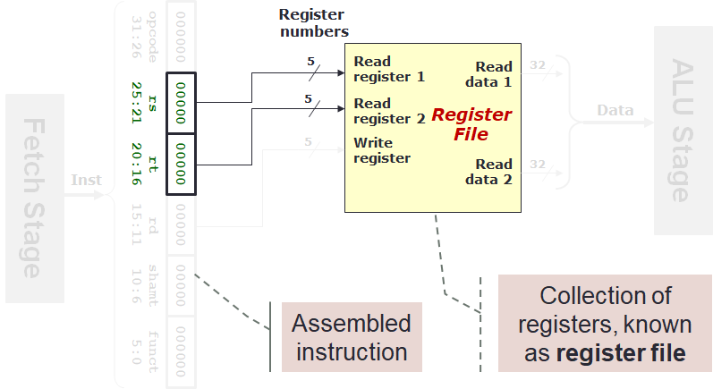
The register number is passed to Register File.
Since there are 32 registers, the number of bits here is 5 bits.
The value of $rs is passed to Read Register 1 and $rt is passed to Read Register 2.
$rs↝Read Register 1$rt↝Read Register 2
Using the register number, the registers are read using the following mapping:
$rs↝Read Register 1↝Read Data 1$rt↝Read Register 2↝Read Data 2
Examples
In these examples, we will use the notation Inst[Y:X] to mean the bits from the instruction Inst from bit X to bit Y.
R-Format Instruction
Consider the instruction add $8, $9, $10.
Its machine code is 0000 0001 0010 1010 0100 0000 0010 0000.
Now we can trace the execution to see if our design works.
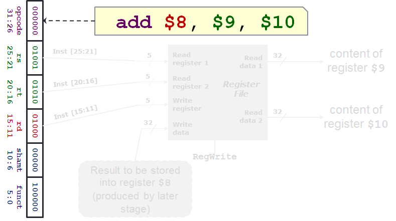
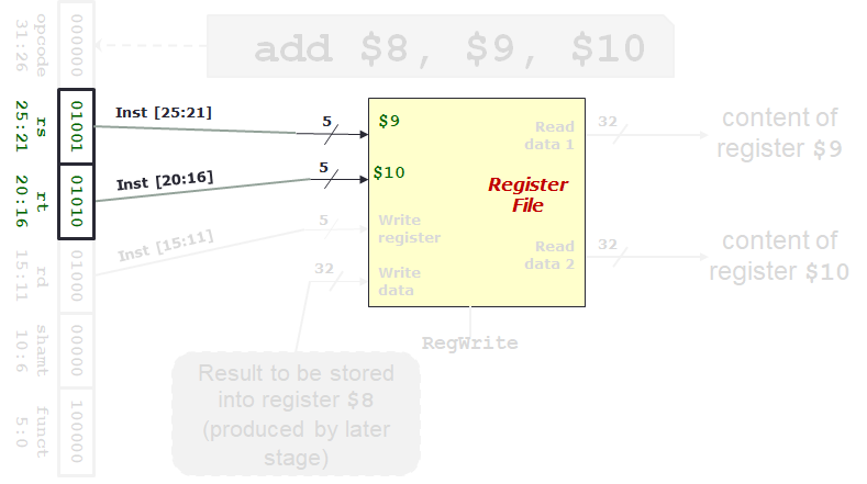
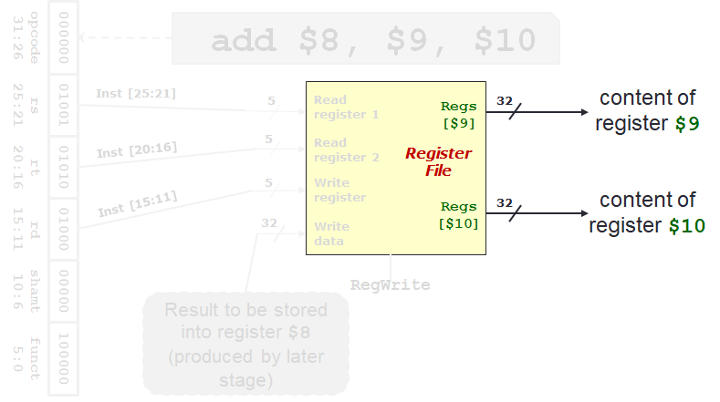
As we have seen, the initial design works for R-format instruction.
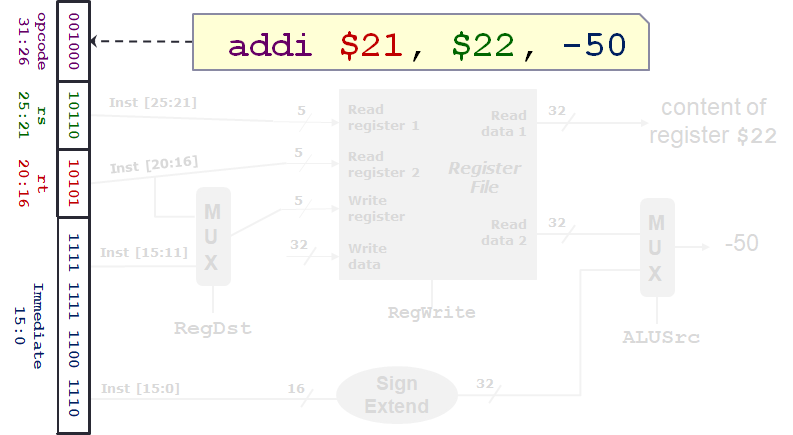
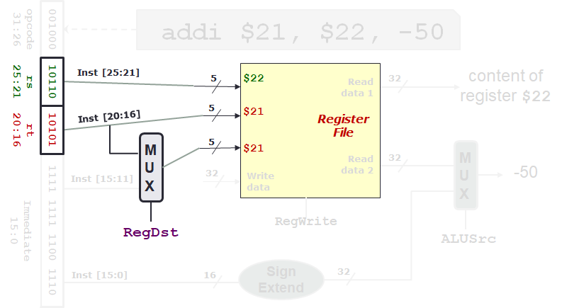
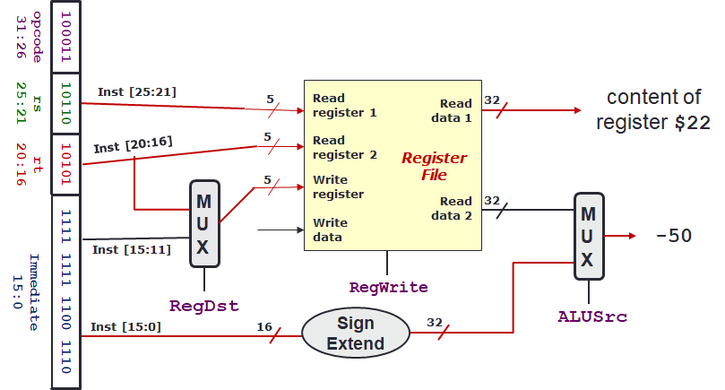
I-Format Instruction
Consider the instruction addi $21, $22, -50.
Its machine code is 0010 0010 1101 0101 1111 1111 1100 1110.
Now we can trace the execution to see if our design works.
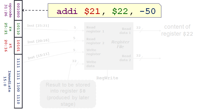
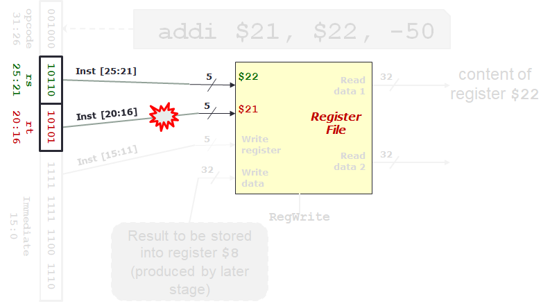
Problems
Using our current initial design, we encounter the following problems:
-
Destination
$21is in the "wrong position".- It should be connected to
Write Register.
- It should be connected to
-
Read Data 2should be from immediate value and not from register.
To solve the problem above, we will need to be able to "choose". This can be done using a multiplexer.
Elements
Register File
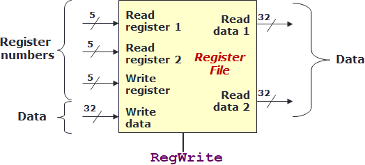
The Register File is simply a collection of 32 registers.
Each of the register is 32-bit wide.
Reading and writing into the register is done by specifying the register number.
We can only read at most 2 registers per instruction (i.e., based on $rs and $rt) and can only write at most 1 register per instruction (i.e., based on $rd or $rt according to instruction).
But what data are we writing?
The Register File we have shown above is incomplete.
We will need to 2 more inputs:
Write Data: The 32-bit data to be written to the register specified byWrite Register.RegWrite: A control signal to indicate whether we want to write into the register or not.- Write:
1ortrue - No Write:
0orfalse
- Write:
Now, for the functional view of a Register File, it is easier to represent it as 2 functions: 1 function to generate the two output and 1 function to write into the register.
Additionally, we can represent the 32 registers as a single-dimensional array similar to Instruction Memory but a much smaller size is needed.
We are going to abuse the function notation to allow returning two values using a notation [val1, val2] with a type of [type1, type2].
These may be extended into more values.
| Functional Conceptual View of Register File | |
|---|---|
1 2 3 4 5 6 7 8 9 10 11 12 13 | |
Multiplexer
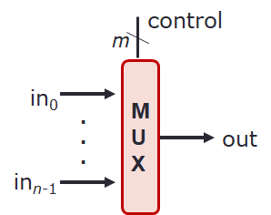
Note that we currently do not have a multiplexer (usually abbreviated as mux) in our diagram, but it is needed to create the correct diagram for the processor.
A multiplexer is another combinational logic but now it is used to select which input is passed to the output.
The block diagram is shown on the right. Again, we can view it conceptually as a function instead. Now, instead of just an input and output, we add another line called the control line1.
-
Inputs
- n inputs in0 to inn-1 shown by an arrow going in to the multiplexer.
- Each input should be the same width.
-
Outputs
- One output out shown by an arrow going out of the multiplexer.
- The result is one of the inputs.
-
Control
- One control with a width of log2 n shown by the control line at the top (sometimes at the bottom).
- This controls which input is selected to the output.
| Functional Conceptual View of Multiplexer | |
|---|---|
1 2 3 4 5 6 7 8 9 10 11 12 13 14 15 16 | |
Sign Extend
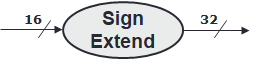
This is the most straightforward combinational logic. It will simply duplicate the MSB of the input until the output is 32 bits wide.
| Functional Conceptual View of Sign Extend | |
|---|---|
1 2 3 4 5 6 7 8 9 | |
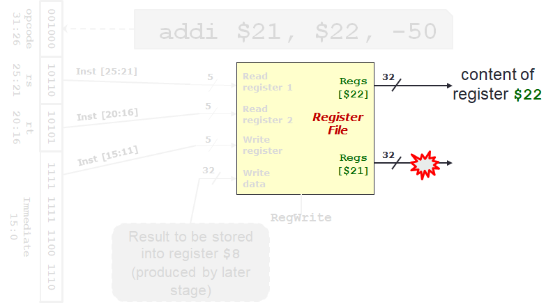
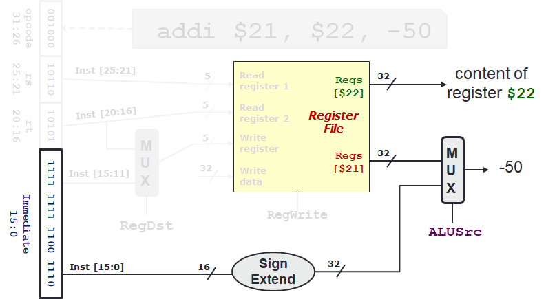
Modified Block Diagram
Using multiplexer, we can modify the block diagram to correct the behaviour for I-format.
There are now two additional multiplexers and one additional sign extend. Furthermore, there are 3 control signals:
-
RegDst: Select which input goes intoWrite Register.Inst[20:16]:0Inst[15:11]:1
-
RegWrite: WriteWriteDatainto register specified byWriteRegisteror not.- No Write:
0 - Write:
1
- No Write:
-
RegDst: Select which input goes into output result.Read Data 2:0Inst[15:11]:1
Using this modified block diagram, the previous problem with I-format instruction no longer pose any problem.
I-Format Instruction
Consider the instruction addi $21, $22, -50.
Its machine code is 0010 0010 1101 0101 1111 1111 1100 1110.
Now we can trace the execution to see if our design works.
Exercise
Do we need a different datapath design for the following instructions?
If not, fill in the missing data (i.e., the ???) and highlight the datapath taken with red colour.
lw $21, -50($22)beq $9, $0, 3
There is no need to modify the datapath.
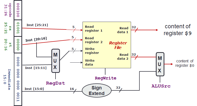
Note that for question 2, we will actually need to calculate both the branch outcome and target at the same time.
We will tacklet his problem at the ALU stage.
For now, simply note that we choose the content of register $0 as our second result because the immediate value is used for computing the target which is simpler than determining the branch outcome.
-
You may think of a control line as just another input. ↩