Fetch Stage
Requirements
The fetch stage does not only fetch the instruction but also prepare the processor to get the next instruction.
-
Use the program counter or
$PCto fetch instruction from memory.$PCis implemented as a special register in the processor.
-
Increment the
$PCby 4 to get the address of the next instruction.$PC+ 4 is the next instruction due to word-alignment.- Exception is made when branch/jump instruction is executed.
-
The instruction is given as output to the next stage (i.e., decode stage).
Block Diagram
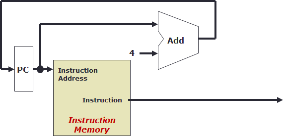
Given the requirements above, we can have the following design:
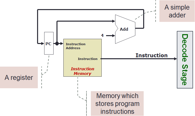
Let us look at the three steps more closely and how they are being satisfied.
Steps
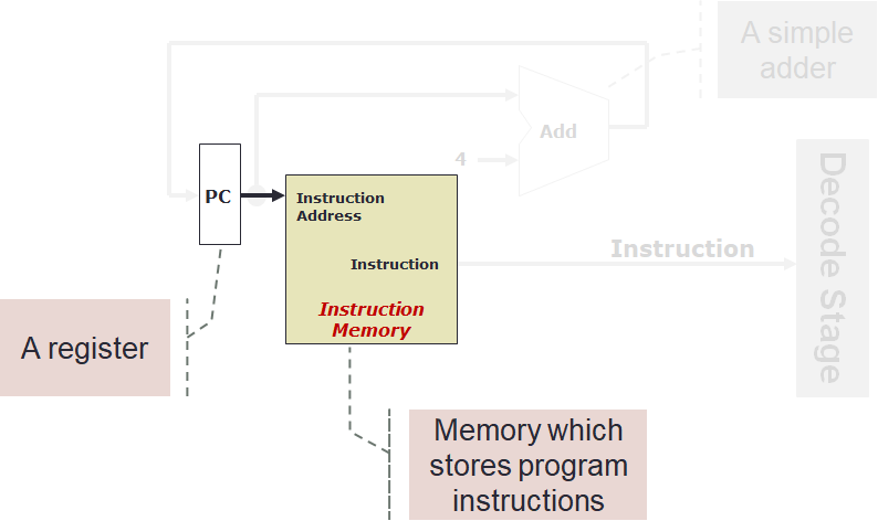
The address of the instruction to be fetched is stored in $PC.
This value is passed to Instruction Address input of the Instruction Memory.
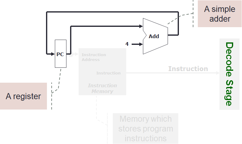
The value inside $PC is incremented by 4 using the adder marked as Add.
This value is passed back to $PC to prepare for the next instruction.
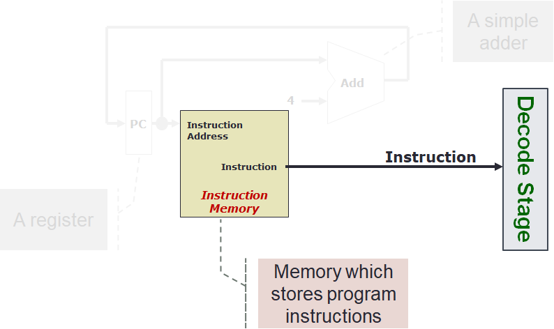
Using the address value from $PC, the Instruction Memory reads the instruction from the memory.
This value is then passed to the next stage (i.e., decode stage).
Clock
There is a slight potential problem when we try to combine "Step 1" and "Step 2" above.
In "Step 1", we are reading the value of $PC but in "Step 2" we are updating the value of $PC.
How can we do both at the same time?
How can it works properly?
The solution is to use a clock.
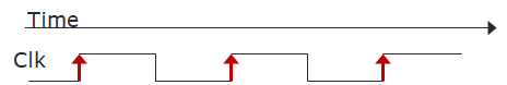
We simply define a clock as "something" that repeats at a regular interval. In the context of processor and circuit, it can be abstracted into a regular signal as seen on the right. Here, you see that the arrow up appears at regular time interval.
There are several convention about a clock.
The convention we use for this current implementation is to read the value of $PC during the first half of the clock period and update the value of $PC with $PC + 4 at the next rising clock edge.
Elements
Instruction Memory
Instruction Memory is a storage element for the instructions1.
This is a sequential circuit which will be covered later.
It has an internal state that stores information as well as clock signal.
The clock signal is not shown and assumed to exist.
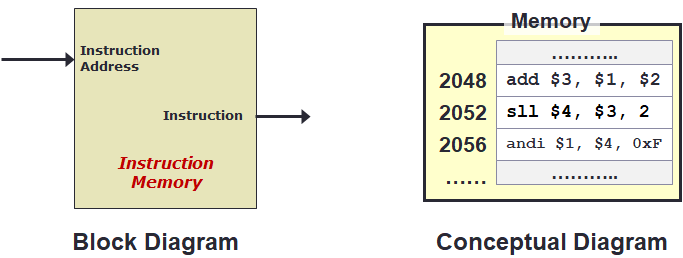
We can view the Instruction Memory as a block diagram or conceptual diagram.
Alternatively, it might be easier to visualise it as a function.
When the function receive an argument M which is an address, it returns the content at address M.
Here, we assume that M is word-aligned.
The internal state can be represented by a single-dimensional array Inst.
| Functional Conceptual View of Instruction Memory | |
|---|---|
1 2 3 4 5 6 7 8 | |
Adder
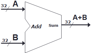
An adder is a combinational logic to implement the addition of two numbers. The block diagram is shown on the right. Again, we can view it conceptually as a function instead. We can describe the function simply by its inputs and outputs as the adder has no internal state due to it being a combinational logic.
-
Inputs
- Two inputs A and B shown by two arrows going to the adder.
- Each input is a 32-bit numbers shown by a slash and the number 32 on the input line.
-
Outputs
- One output A+B shown by an arrow going out of the adder.
- The result is a 32-bit numbers shown by a slash and the number 32 on the output line.
| Functional Conceptual View of Adder | |
|---|---|
1 2 3 4 5 6 7 | |
-
Here we slighly deviate from the standard von Neumann architecture because this memory unit only retrieve instructions. ↩